What is the Importance of Via-in-Pad in HDI PCB?
In the world of modern electronics, High-Density Interconnector (HDI) PCBs have become the backbone of innovation, offering unparalleled miniaturization, high performance, and design flexibility. HDI PCBs are essential in devices like smartphones, wearables, and medical instruments, where space constraints are crucial. One of the key features that make HDI PCBs so effective in advanced electronics design is the use of via-in-pad technology. But what exactly is via-in-pad, and why is it so important in HDI PCB design?
Understanding Via-in-Pad Technology
A via-in-pad refers to a manufacturing technique in which a via (a small hole that allows electrical connections between different layers of the PCB) is placed directly inside a pad—typically a surface mount pad used for components like ICs (Integrated Circuits). In traditional PCBs, vias are drilled outside the pad area to avoid any interference with the placement of components. However, hdi pcb designs often require very tight spacing, making traditional methods challenging.
By integrating the via directly into the pad, engineers can significantly save on space. This method is particularly useful when dealing with high-frequency designs and tight-pitched components, where real estate on the PCB is limited.
The Role of Via-in-Pad in HDI PCBs
The importance of via-in-pad in HDI PCBs lies in its ability to address the evolving demands of modern electronics. Here are some key reasons why via-in-pad technology is essential:
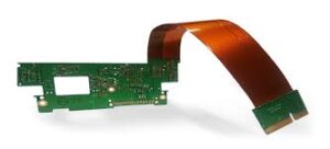
Space Optimization: As consumer electronics continue to get smaller and more powerful, the need for compact PCB designs has never been higher. Via-in-pad allows designers to place components more densely, increasing the overall component count and reducing the size of the PCB. This is crucial for devices where real estate is at a premium, such as wearables, mobile devices, and medical gadgets.
Improved Signal Integrity: In HDI PCB designs, the performance of high-speed signals can be affected by factors like trace impedance and signal routing. Via-in-pad helps minimize the distance between components, reducing the potential for signal degradation. This improvement in signal integrity is essential for applications where precise data transmission and high-frequency performance are critical.
Enhanced Reliability: Traditional vias, when used in close proximity to pads, can lead to reliability issues such as pad lifting or damage during assembly or rework. Via-in-pad designs help mitigate these problems by creating a more stable structure. Additionally, by using specialized via-fill techniques, the vias can be filled with conductive or non-conductive materials, reducing the risk of damage during the manufacturing process.
Facilitates Microvia and Blind Vias: HDI PCBs often incorporate microvias and blind vias, which are smaller and more precise than traditional vias. Via-in-pad technology is particularly beneficial when integrating these small vias, allowing for better layer transitions and reduced PCB thickness, which is essential for creating multi-layered, high-density interconnects.
Cost-Effective Manufacturing: Despite the challenges of integrating vias into pads, the benefits of via-in-pad technology often outweigh the costs. The enhanced compactness of the design reduces the need for larger PCBs, which helps reduce overall production costs. Additionally, fewer layers and components can simplify the assembly process, improving efficiency.
Conclusion
Via-in-pad technology plays a vital role in the performance and manufacturability of HDI PCBs. By enabling designers to optimize space, enhance signal integrity, and improve reliability, via-in-pad makes it possible to meet the demands of today’s cutting-edge electronic devices. As the need for smaller, faster, and more efficient devices grows, the role of via-in-pad technology in HDI PCB design will continue to be critical in driving innovation across various industries.