Pcb Board Assembly Manufacturing Vary Across Industries
The pcb board assembly manufacturing process is highly orchestrated, and the final product is dependent on every one of its parts to work as intended. A series of automated inspections harmonize with visual inspections to ensure that the board adheres to strict quality standards throughout production.
This is why a thorough understanding of the PCB assembly process is essential for all stakeholders involved in the manufacturing chain, from design engineer to end user. Getting the initial design right is key to a successful PCB that works as intended. For this reason, many companies specializing in PCB assembly offer a service called design for manufacturability (DFM) checks, where they review the design file to identify any issues that may prevent the board from advancing through the fabrication process.
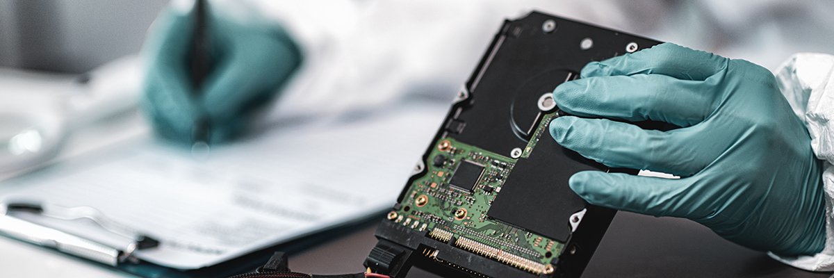
Once the bare boards have been fabricated, the next step in the process is component placement. Automated pick-and-place machines, equipped with vacuum nozzles and precision robotic arms, carefully pick up components from their packaging and place them on the substrate according to the design blueprint. This step is vitally important, as even a slight misalignment can lead to subpar connections or even a short circuit.
After the components have been placed, the assembly process moves on to soldering, a process that forges the critical electrical and mechanical bond between the components and the PCB. The soldering step can be performed through a variety of methods, including wave and reflow soldering. Both of these processes involve heating a metal alloy to the point where it melts, creating a strong connection between the components and the board.

How Does Pcb Board Assembly Manufacturing Vary Across Industries?
In the final stage of PCB assembly, the board undergoes a thorough inspection and testing to check for misalignments and subpar solder connections. This can be done through various methods, including automatic optical inspection (AOI), which uses a series of high-powered cameras arranged at different angles to view the solder connections and their quality. AOI machines are able to recognize low-quality connections because they reflect light differently than high-quality connections.
After the final inspection, the board is ready for shipment to its end user. Before this, it must undergo a rigorous washing cycle in which it is washed with deionized water. This is because the ions in regular water can cause problems in electronic devices. Deionized water, on the other hand, poses no threat to the components.
Then, the PCB is inserted into its enclosure, which will protect it from damage and environmental hazards. This is the final step of the PCB assembly process, and it allows for more efficient shipping and storage of the device. In addition, the enclosure will help protect the circuit from electromagnetic interference, which is common in industrial environments. This way, the device will continue to function as intended for its entire lifespan.
Inspection techniques provide valuable data that can be used to optimize the manufacturing process. By analyzing inspection results, manufacturers can identify patterns and recurring issues, enabling them to make informed decisions about process adjustments and improvements. For instance, if a particular type of defect is frequently detected, the root cause can be investigated, and process parameters can be adjusted to mitigate the issue. This continuous feedback loop helps in maintaining high production yields and enhancing overall process efficiency.