purpose of an high density interconnect pcb
The use of high-density interconnect (HDI) technology in PCB design allows for more intricate designs to be built in a smaller, more compact package. This helps to reduce weight and size without sacrificing performance. HDI is increasingly being used in consumer electronics, including wearable devices and virtual reality headsets. It is also being incorporated into military and aerospace systems due to its ability to withstand extreme environments and hazardous conditions.
high density interconnect pcb offer a number of key benefits, including higher wiring density and lower layer counts. They can also be fabricated using more expensive materials such as polyimide, allowing for more advanced features to be implemented in a smaller space. This can reduce costs and lead to a more competitive finished product.
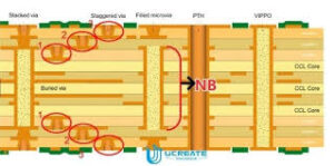
Another benefit of HDI is that it can be designed to support higher pin-count components, resulting in reduced thermal and signal integrity issues. This is achieved through the use of smaller trace widths and spacing, as well as by implementing blind and buried via technologies. These techniques allow for routing channels on inner layers to be established that do not require the drilling of through holes, thereby saving valuable board real estate.
What is the purpose of an high density interconnect pcb?
These new technologies and design methodologies are enabling designers to develop more complex electronic products that better meet modern technological demands. However, the increased circuitry and interconnections associated with HDI PCBs can add significant complexity to the design process. This increases the need for highly skilled multidisciplinary teams of electrical engineers, mechanical engineers and manufacturing experts to work together to successfully implement the necessary design changes.
The development of HDI boards requires careful consideration of the component selection. This will determine the routing widths, locations, and types of drilled holes, as well as the stack-up. In addition, the choice of material type and the number of layers will have a direct impact on manufacturing cost.
One of the main challenges of designing an HDI PCB is ensuring that the signal propagation paths are consistent with the impedance requirements of each digital, analog and power signal. This can be accomplished by ensuring that the shortest trace lengths are used for each signal, and by providing sufficient ground planes for the signals.
The manufacturing of HDI PCBs is a complex and time-consuming process, which requires specialized equipment. The process begins with photoresist deposition and exposure, followed by etching and removal of the resist. The remaining conductor patterns are then etched into the laminate, and the plated with copper. The vias are then defined using either contact imaging or laser drill, and they are etched through the laminate to create the required connections. In order to reduce the amount of drooping that can occur during the drill process, a “via-in-pad” technique is employed.
The final step in the fabrication process involves putting the layers of the PCB stackup together. This is usually done by multiple lamination cycles, and the outer layers are then metallized. This step is a critical part of the assembly, since it can affect the performance and reliability of the final product.